 Book a call
Cut. Drill. Pattern.
Without heat.
Femtosecond cutting, microdrilling, selective thin-film removal, surface texturing, and maskless patterning in glass, wafers, ceramics, sapphire, metals, polymers, and composites.
Micron-scale control for cuts, holes, grooves, apertures, textures, and selective layer removal.
Zero heat in surrounding material
Cuts, holes, slots, and patterns
Selective removal and texturing
Microscopy and interferometry
More than a cut.
A new design space.
Create micron-scale openings, isolate thin films, texture functional surfaces, resize active wafers, shape hard crystals, and machine material stacks without masks or hard tooling.
Glass & crystal shaping
Cut freeform outlines, scribe controlled separation lines, drill optical ports, open fluidic channels, texture surfaces, and resize brittle crystals with zero heat and zero tool contact.
Explore capability ↗Active wafer processing
Shape active device wafers, open sensor and MEMS features, resize photonic substrates, form isolation cuts, and create nonstandard die geometries with programmable, contact-free toolpaths.
Explore capability ↗Precision metal features
Form slots, apertures, flexures, meshes, electrodes, isolation cuts, and intricate outlines with zero heat distortion and zero tool wear.
Explore capability ↗Polymer film conversion
Convert polyimide, PEEK, PET, adhesive stacks, diagnostic films, flexible circuits, sensor layers, and composite laminates without dies or mechanical contact.
Explore capability ↗Microholes & apertures
Create circular and noncircular holes, tapered bores, nozzle arrays, fluidic ports, vents, slots, fiducials, and electrical isolation features across material classes.
Explore capability ↗Selective layer ablation
Remove coatings and metallization, isolate conductive layers, expose buried materials, write sensor patterns, and texture functional surfaces with programmed depth and geometry.
Explore capability ↗Capability,
documented.
Parameter maps, microscope images, white light interferometry, feature measurements, and process notes turn an ultrafast laser result into a repeatable manufacturing process.
Explore qualification packages ↗- Define
Specify the material stack, feature geometry, depth, edge, and surface requirements.
- Program
We map pulse energy, repetition rate, scan strategy, focus, and toolpath.
- Machine
Cold ablation forms the feature with zero mechanical contact and zero heat.
- Measure
Microscopy and white light interferometry document geometry and surface structure.
- Scale
The qualified process moves from coupons to prototypes and pilot lots.
From optical crystals
to active devices.
Cold ablation machines transparent, brittle, conductive, flexible, coated, crystalline, and composite materials with zero thermal load.
- Glass
- Fused silica & quartz
- Sapphire
- Silicon
- Ceramics
- Compound semiconductors
- Active device wafers
- Thin metals & foils
- Polyimide & polymer films
- Composites
- Coated substrates
- Thin films & metallization
Zero heat. Zero force.
Micron-scale control.
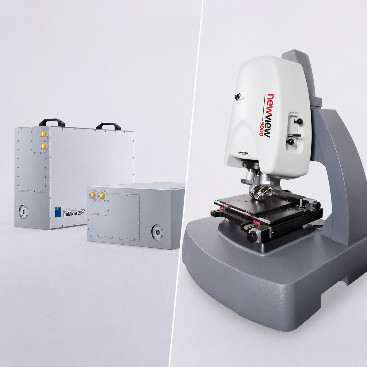
Our TRUMPF TruMicro 2030 industrial platform delivers 1030 nm cold ablation for precision ultrashort-pulse cutting, drilling, patterning, selective removal, and surface structuring.
- Wavelength
- 1030 nm infrared
- Pulse duration
- 900 fs operation
- Process types
- Cold cutting · scribing · drilling · ablation · patterning · texturing
- Geometry
- Through-cuts · blind features · tapered holes · selective layers · 3D surfaces
- Inspection
- Optical microscopy · white light interferometry · dimensional measurement
- Wafer size
- Up to 100 mm today · planned support over 300 mm by Q1 2027
Put a new geometry
on the table.
Send the material stack, drawing, feature depth, quantity, and surface requirements. We’ll map the cold-ablation process and inspection plan.